
From Speculative to Strategic: When MEMS and MOEMS Became Mainstream
For decades, Microelectromechanical Systems (MEMS) and Micro-Optoelectromechanical Systems (MOEMS) occupied a liminal space in semiconductor discourse. Their promise was undeniable: tiny mechanical elements on chips that could sense, actuate, and communicate. But their integration into mainstream roadmaps always felt just out of reach. Now, thanks to a shift in mindset and infrastructure, MEMS and MOEMS have crossed a threshold. Erik Hosler, a respected semiconductor strategist and longtime EUV expert, observes that their emergence is a sign of a larger transformation in how the industry asks questions and finds answers.
The recent SPIE Advanced Lithography conference made this shift explicit. Long considered fringe or exploratory, MEMS and MOEMS were featured not as novelties but as essential components of tomorrow’s architectures. It wasn’t a matter of novelty for novelty’s sake. These devices are increasingly vital to applications ranging from sensing and imaging to quantum experimentation and on-chip communication.
A Seat at the Table
What changed? Part of it is technological maturity. Fabrication techniques have improved, cost barriers have lowered, and integration with CMOS platforms has become more feasible. But the bigger shift is philosophical. The industry is no longer solely chasing shrinkage or speed. Instead, it is chasing functionality, especially functionality that crosses traditional disciplinary boundaries.
This new emphasis has opened the door for systems that combine electrical, mechanical, and optical capabilities in novel ways. MEMS-based inertial sensors and pressure gauges were just the beginning. Today, we are seeing MOEMS elements used in beam steering for LiDAR, tunable photonics, and quantum interfaces. These are not speculative ideas, but strategic responses to real engineering problems.
Signals of Strategic Inclusion
At the SPIE Advanced Lithography conference, the conversation about MEMS and MOEMS was no longer speculative. Their inclusion signaled a deliberate broadening of the technological lens used to shape the future of the semiconductor roadmap.
This new direction was captured in an observation from the conference. Erik Hosler says, “Last year, we included MEMS and MOEMS, and we will keep expanding to quantum to make this a place to ask questions … Lots of great things are going on, and something will emerge.”
This comment, made in the context of expanding SPIE’s technical scope, underscores the growing importance of intellectual openness. The goal is not to push any one niche technology as a panacea, but to create a platform for exploration. The strategic value lies in SPIE’s willingness to host early-stage conversations that may guide tomorrow’s breakthroughs.
Enabling New Architectures
The inclusion of MEMS and MOEMS is not just an incremental addition, but marks a significant shift in how semiconductor systems are conceptualized and designed. These devices allow new kinds of architectures that would have been difficult or impossible with purely electronic systems. Consider dynamic tuning: MEMS actuators can adjust physical positions with extreme precision, enabling real-time reconfiguration of optical paths or resonance conditions. This reconfigurability is crucial for edge AI, adaptive optics, and even quantum signal processing.
Such integration also changes the layout and tooling demands for advanced lithography. Patterning techniques must now accommodate moving structures and variable alignment tolerances. It is a new layer of complexity, but also one full of creative potential. Lithographers are being asked to design not just for stability but for intentional flexibility.
A Broader Horizon for Fabrication
The adoption of MEMS and MOEMS is also reshaping how fabs people think about capability. In the past, specialized foundries handled these devices. Now, major fabs are beginning to explore multi-functional process flows that include MEMS steps. It means new masks, new etch processes, and greater cross-disciplinary collaboration within cleanrooms.
It also demands new metrology approaches. Standard wafer inspection tools may not capture the nuances of mechanical performance or optical path accuracy. As a result, hybrid measurement systems that combine interferometry, surface profilometry, and machine vision are seeing more interest.
Education and Talent Strategy
Making MEMS and MOEMS mainstream requires tools and people, and training programs are shifting accordingly. Engineers who once specialized in photonics or mechanical systems are now learning the basics of CMOS compatibility and mask layout. Conversely, traditional semiconductor engineers are being introduced to new models of motion, fluidics, and photon interaction.
Some universities are offering joint degrees or certifications that span EE, ME, and applied physics. Internships are being restructured to ensure that exposure to MEMS tooling is part of a standard rotation. This blending of disciplines is helpful and essential for the future of integrated development.
Implications for the Roadmap
The inclusion of MEMS and MOEMS in strategic planning has ripple effects. It challenges assumptions about what constitutes a “core” technology. It invites collaboration with nontraditional partners, including those from aerospace, medical technology, and instrumentation. It also prompts a rethinking of what success looks like. Smaller feature sizes may still matter, but so do broader functionality and system-level adaptability.
Importantly, MEMS and MOEMS also connect to the future of quantum devices. Many quantum systems require precise mechanical or optical alignment, which MEMS and MOEMS are uniquely suited to handle. They could become the bridge between today’s classical chips and tomorrow’s quantum platforms.
From Fringe to Framework
As MEMS and MOEMS continue their rise, it is important to recognize that their integration will not follow a uniform path. Use cases will vary widely depending on application requirements, technological capabilities, and ecosystem support. Some fabs will embrace them fully, integrating them with EUV flows. Others may specialize in hybrid packages or chiplets that connect separate domains. What unites these paths is a willingness to ask new questions and the openness to rethink how semiconductor innovation is defined.
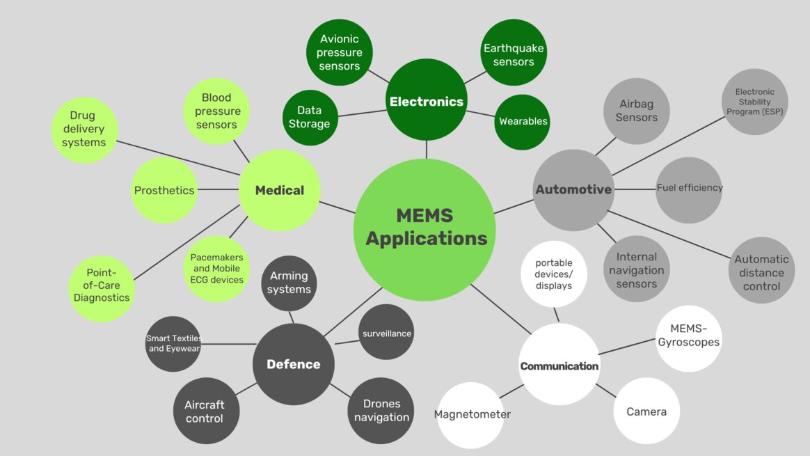
We may also see MEMS and MOEMS expand into sectors not traditionally tied to advanced lithography, including wearables, energy harvesting systems, and biomedical platforms. These extensions will further illustrate the adaptability and relevance of these systems as the industry continues to develop.
At SPIE and beyond, the message is clear: the future will not be delivered by electronics alone. It will come from systems that see, feel, move, and adapt. MEMS and MOEMS are no longer speculative. They are strategic. Their presence signals a new chapter in semiconductor innovation, one where complexity is not just tolerated but embraced. And if history is any guide, these once-sidelined technologies may just become the heart of the next big leap.